Multilayer PCB (printed circuit board) is widely used for multi-layer circuit wiring and connection in electronic devices. Its main uses include but are not limited to the following points:
First, multilayer PCB allows more complex circuit design in a limited space. By increasing the number of layers, designers can arrange circuits and signals between different layers, thereby
reducing mutual interference and improving signal integrity. This is particularly important in high-frequency and high-speed applications, such as computers, communication equipment, and high-end consumer electronics.
Second, while providing electrical isolation, Multiply-Layer Rigid PCB can also effectively reduce the overall size and weight of the circuit board. For small electronic devices such as smartphones, tablets, and embedded devices, multilayer PCBs can support complex functions without taking up too much space, which helps to design lighter and more portable products.
In addition, multilayer PCBs also increase the flexibility of the manufacturing process. Designers can distribute different functional modules in different layers to facilitate subsequent assembly and testing. Especially in areas such as automotive, medical electronics, and industrial control that require reliability and stability, the high durability and high-density wiring advantages of Multiply-Layer Rigid PCB are particularly prominent.
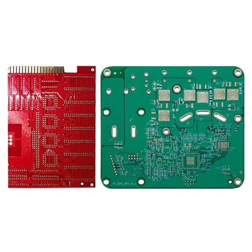
The biggest difference between Multiply-Layer Rigid PCB boards and single-sided and double-sided boards is the addition of internal power and ground layers. The power and ground networks are mainly routed on the power layer. On PCB multilayer boards, there is conductive metal on both sides of each substrate layer, and special adhesives are used to connect the boards together, and there is insulating material between each board. However, PCB multilayer wiring is mainly based on the top and bottom layers, supplemented by the middle wiring layer. Therefore, the design of Multiply-Layer Rigid PCB boards is basically the same as the design method of double-sided boards. The key is how to optimize the wiring of the internal electrical layer to make the wiring of the circuit board more reasonable. The inevitable product of multifunctional development, large capacity and small volume.
PCB is a circuit board manufactured in a similar way to printing, so common PCBs are bonded together in several layers, and each layer has a resin insulating substrate and a metal circuit layer. The most basic PCB is divided into 4 layers. The top and bottom circuits are functional circuits, arranging the most important circuits and components, and the middle two circuits are ground layers and power layers. The advantage is that it can make corrections to the signal lines and better shield interference. Generally speaking, 4 layers are enough for the normal operation of the PCB, so the so-called 6 layers, 8 layers, and 10 layers are actually adding more circuit layers to improve the electrical capacity of the PCB, that is, the pressure bearing capacity.
Therefore, the increase in the number of PCB layers means that more circuits can be designed inside. For memory, when do you need to increase the number of PCB layers? According to the above, it is obviously when the electrical power of the PCB is too strong or too high. When is the voltage and current of the memory PCB the strongest? Players who have played overclocking will know that if the memory wants to achieve better performance, it must be pressurized to increase the operating frequency. Therefore, it is not difficult for us to conclude that when the memory can be used at high frequency or overclocked.